
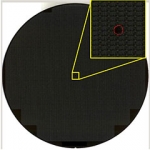
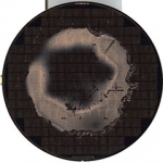
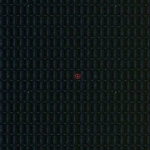
Wafer Hotspot Defects A hotspot macro defect is a localized area that is out of focus and may...
Microtronic, Inc. Contact Us: 1-877-642-7687 | 1-508-627-8951 [email protected]
Wafer Hotspot Defects
- Home
- Wafer Hotspot Defects
Author Archive


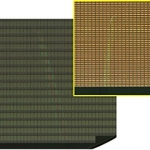
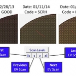
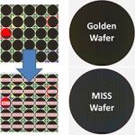
First 12 Wafers – Different Occasionally half of the semiconductor wafers in a lot that are inspected are...

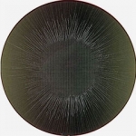
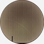
Flashfield Defects Flash field defects are typically near the edge of the semiconductor wafer and due to a...

Wafer Edge Discoloration EAGLEview image of a semiconductor wafer with a discoloration macro defect on the edge of...

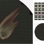
Developer Related Defects Semiconductor wafer macro defect caused by poor develop or a poor rinse during the wafer...

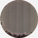
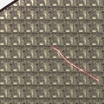
EBR Drip Defect EBR drip, sometimes called the “eyelash” semiconductor wafer macro defect, may occur at a very...

Wafer Contamination – Small EAGLEview detects small contamination defects on the semiconductor wafer instantly. Typically, any small semiconductor...

Wafer Contamination – Large An example of a large contamination macro defect found by EAGLEview on a semiconductor...

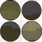
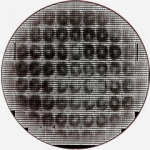
CMP – Macro Defects Several examples of CMP related macro defects detected during an EAGLEview inspection run There...

Edge Chips – Macro Defects Above is an example of a semiconductor wafer edge chip defect detected by...
Download Microtronic Macro Defect Brochure
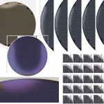
Gallery of Macro Defects Detected By EAGLEview
Contact Us Today
Microtronic is a leader in Semiconductor Wafer Defect Inspection, Sorting and Metrology.